Samsung chief Lee visits Japan chip packaging lab
 Story summary
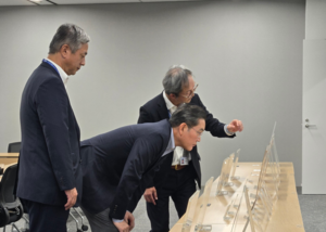
Samsung Electronics Executive Chair Lee Jae-yong visited the company's advanced semiconductor packaging research facility in Japan on Sunday, emphasizing the need to secure cutting-edge packaging technologies to sharpen its competitive edge in AI chips. Lee inspected the Advanced Package Lab in Yokohama, where he re…
Read at The Korea HeraldOpens the original publisher in a new tab. Full articles belong to their publishers; a subscription may be required.